
GPIO14 - General Purpose I2C I/O Expansion Chip
Introduction
The GPIO14 chip is a pre-programmed PIC16F818 running on an
internal 8MHz clock. It is intended to provide general purpose I/O expansion on
the I2C bus.
In this document you will find:
Features
GPIO14 Pin Connection Diagram
Internal Registers
Commands
Analogue to Digital (A/D)
Conversion
PWM Output
Ultrasonic Ranging
Changing the I2C Bus Address
Features Include;
Up to 2 SRF04's or 2 SRF05's controlled, including all timing.
Up to 14 general purpose Input/Output lines.
Up to 5 Analogue input channels with 10-bit A/D conversion.
1 PWM output usable as an 8-bit D/A with a simple filter.
I2C address 0x40, can be changed to allow up to 8 devices on the same I2C bus.
6 I/O lines have programmable pull-up resistors built into the chip .
Individual control of each pin for Input or Output.
Simple commands for Bit Set, Bit Clear and Bit Toggle.
Easy I2C bus control, similar protocol as popular EEPROM's such as 24C02.
Connection Diagram showing GPIO14 Pin connections.

The GPIO14 requires a 5v power supply. Current consumption is very low - around 2mA. A 100n capacitor should be connected between the 5v supply and Ground close to the chip. I2C is connected to SDA (pin7) and SCL (pin 10). You should have pull-up resistors on the SDA and SCL lines. A value of 4k7 is normally OK. We use 1k8 resistors for better noise immunity, but anything from 1k8 to 10k should be OK. You only need one pair of pull-up resistors on the whole I2C bus, not for each device. The pull-up resistors are normally located on the bus master. Our CM02 already has 1k8 resistors fitted on the module.
There are two 8-bit ports on the GPIO14. Port A and Port B. The individual bits in Port A are RA0 to RA7, and for Port B they are RB0 to RB7. Only 6 of these are available because RB1 is used for the SDA line and RB4 is used for the SCL line. You can still write anything you wish to Port B though, because the firmware will prevent the I2C lines from being overwritten. Bits RB0, RB2, RB3, RB5, RB6 and RB7 are available for general purpose I/O. Some pins can have other functions. RA0 to RA4 can be used for analogue inputs. RB3 can be used as a PWM output. Bits RB0, RB2, RB3, RB5, RB6 and RB7 can have a pull-up resistor enabled. RA5 is an input only pin, this is a limitation of the PIC16F818 used. All I/O lines default to inputs on power up.
Internal Registers
The GPIO14 has eight internal registers, some of which have different functions
for read and write.
| Register | Read | Write |
| 0 | Firmware Revision Number | Command Register |
| 1 | Result high byte | Port A Input/Output Mask |
| 2 | Result low byte | Port B Input/Output Mask |
| 3 | A/D Control | A/D Control |
| 4 | Port A | Port A |
| 5 | Port B | Port B |
| 6 | PWM | PWM |
| 7 | Nothing (Reads Zero) | I2C Address Change |
Register 0
When reading from the GPIO14, register 0 will return the Firmware revision
number (currently 2 at the time of writing - November 2005). Writing to register 0 writes to the command register.
This is used to Set, Clear and Toggle the I/O pins and a few other commands.
Full details are in the Commands section below.
Registers 1 & 2
Reading from these registers will return the result register. This 16-bit
register holds either the result of the most recent A/D conversion (Full details are in
the Analogue to digital section below) or the most
recent ultrasonic ranging (Full details are in the Ultrasonic
Ranging section). Writing to these
registers writes to the Port direction control registers. Each bit that is set
makes the port pin an input. Clearing a bit make the pin an output. For example
writing 1 (0x01 hex or 00000001 binary) to register 2 will make Port B bit 0
(RB0) an input and all the other port B bits an output. Note - as RA5 can only
be an input pin, bit 5 is ignored when writing to register 1. Also RB1 and RB4
are dedicated to the I2C bus, therefore bits 1 and 4 are ignored when writing to
register 2.
Register 3
This register can be both read and written. It is used to set up which pins
are used for analogue inputs and which are digital. Full details are in the Analogue
to digital section below.
Registers 4 & 5
These are the Port A and Port B data registers. Writing to these registers
will place the data on those port pins which are configured as outputs. Pins
which are inputs will not change, they remain input pins, however, if a pin is
later changed to an output by writing to register 1 or 2, then this data will immediately
be output. Reading from these registers will return the data currently on the
pins, whether they are input or output.
Register 6
Pin 9, port pin RB3, can optionally be used as a pwm output. Writing to this
register sets the 8-bit pwm period. Full details are in the PWM section below.
This register can be read or written.
Register 7
This write only register is used to change the I2C address of the GPIO14
chip from its factory default of 0x40. See the I2C address section below for
details.
Commands
The GPIO14 chip has a complete set of commands to Set, Clear or Toggle the
port pins. Just write one of these values to the command register, the pin will
automatically be set to output regardless of its previous state. RA5 is missing
because it is an input only pin and RB1 and RB4 are missing because they are
dedicated to the I2C bus.
| I/O Pin | Bit Set | Bit Clear | Bit Toggle |
| RA0 | 16 (0x10) | 32 (0x20) | 48 (0x30) |
| RA1 | 17 (0x11) | 33 (0x21) | 49 (0x31) |
| RA2 | 18 (0x12) | 34 (0x22) | 50 (0x32) |
| RA3 | 19 (0x13) | 35 (0x23) | 51 (0x33) |
| RA4 | 20 (0x14) | 36 (0x24) | 52 (0x34) |
| RA6 | 22 (0x16) | 38 (0x26) | 54 (0x36) |
| RA7 | 23 (0x17) | 39 (0x27) | 55 (0x37) |
| RB0 | 24 (0x18) | 40 (0x28) | 56 (0x38) |
| RB2 | 26 (0x1A) | 42 (0x2A) | 58 (0x3A) |
| RB3 | 27 (0x1B) | 43 (0x2B) | 59 (0x3B) |
| RB5 | 29 (0x1D) | 45 (0x2D) | 61 (0x3D) |
| RB6 | 30 (0x1E) | 46 (0x2E) | 62 (0x3E) |
| RB7 | 31 (0x1F) | 47 (0x2F) | 63 (0x3F) |
There are 15 other commands that can be sent to the command register:
| Name | Command | Action |
| NO_OP | 0 (0x00) | No Operation |
| PULLB_ON | 1 (0x01) | Port B pull up resistors active |
| PULLB_OFF | 2 (0x02) | Port B pull up resistors disabled |
| GET_AD0 | 3 (0x03) | Get Analogue Channel 0 (RA0) |
| GET_AD1 | 4 (0x04) | Get Analogue Channel 1 (RA1) |
| GET_AD2 | 5 (0x05) | Get Analogue Channel 2 (RA2) |
| GET_AD3 | 6 (0x06) | Get Analogue Channel 3 (RA3) |
| GET_AD4 | 7 (0x07) | Get Analogue Channel 4 (RA4) |
| GET_S4A | 8 (0x08) | Get Range of SRF04 A |
| GET_S4B | 9 (0x09) | Get Range of SRF04 B |
| GET_S5A | 10 (0x0A) | Get Range of SRF05 A |
| GET_S5B | 11 (0x0B) | Get Range of SRF05 B |
| SET_US | 12 (0x0C) | Set ranging in uS |
| SET_CM | 13 (0x0D) | Set ranging in centimeters |
| SET_IN | 14 (0x0E) | Set ranging in Inches |
All commands not defined in the two tables above will be treated
as NO_OP and will have no effect.
PULLB_ON and PULLB_OFF turn the Port B internal pull up resistors on and off. These are
typically around 20k in value but can vary from 12.5k to 100k.
GET_AD0, GET_AD1, GET_AD2, GET_AD3 and GET_AD4 convert the Analogue channel to
10-bit accuracy and place the result in the RESULT register. The A/D conversion
is very fast. You can send the GET_ADx command and then read the RESULT register
immediately. Commands 8 (0x08) - 14 (0x0E) are for ultrasonic ranging using the
SRF04 or SRF05 modules. Full details of these commands are in the Ultrasonic
Ranging section.
Analogue to Digital (A/D)
Conversion
Five of the GPIO14 pins can be used for analog inputs. These are AN0 to AN4
(pins 17, 18, 1, 2, and 3). Which of these are actually available depends on the
value written to register 3, the A/D control register. The A/D control register
can also be used to set left or right justification of the 10-bit result. Left
justification places the 10-bit result in bits 15-6 of the result register, bits
5-0 will be zero. This is useful if you only need an 8-bit result, as you can
just read it from register 1 (A/D result high byte). Right justification places
the 10-bit result in bits 9-0 of the result register, bits 15-10 will be zero.
The 16-bit result register will therefore contain values from 0 to 1023 (0x0000 to
0x03FF). Set bit 7 of the A/D control register for right justification and
clear it for left justification.
A/D Control Register
| 7 | 6 | 5 | 4 | 3 | 2 | 1 | 0 |
| ADFM | 1 | x | x | PCFG3 | PCFG2 | PCFG1 | PCFG0 |
| Bit7 |
ADFM |
1 A/D result is right justified 0 A/D result is left justified |
|||||||||||||||||||||||||||||||||||||||||||||||||||||||||||||||||||||||||||||||||||||||||||||||||||||||||||||||||||||||||||||||||||||||||
| Bit 6 | 1 | This bit is always forced to a 1 | |||||||||||||||||||||||||||||||||||||||||||||||||||||||||||||||||||||||||||||||||||||||||||||||||||||||||||||||||||||||||||||||||||||||||
| Bits 5,4 | x x | Unused bits - always read 0 | |||||||||||||||||||||||||||||||||||||||||||||||||||||||||||||||||||||||||||||||||||||||||||||||||||||||||||||||||||||||||||||||||||||||||
| Bits 3,2,1,0 |
PCFG |
These bits select which pins will be Analogue, Digital and Reference
voltage inputs.
|
As you can see, there are limitations on which combinations of
Analogue and Digital inputs are possible. Bear this in mind when wiring the chip
up. The four most useful combinations are shown hi-lighted in green. The A/D Control Register must be set up before you do your first conversion.
The GET_ADx commands will automatically make the selected channel an input an
leave it as an input after conversion. If you write to the Port A direction
control register, make sure you keep the required analogue channels as inputs.
A channel is converted by issuing a GET_ADx command, which will place the value
in the result register. You can then get the value by reading the result
register. It therefore requires two separate I2C transaction sequences, one to
issue the command and one to read the result. The VRef+ and VRef- options are
for using your own reference inputs. The conversion is normally for inputs
ranging between 0v and 5v (the highlighted options). By selecting other options
you can convert between 0v and whatever you put on the VRef+ pin, or between
VRef+ and VRef-. Do not put more that 5v or less than 0v onto any pin. The
minimum range for Vref+ - Vref- is 2.5v.
PWM Output
Pin 9, port pin RB3, can optionally be used as a PWM output. A very simple
filter will make this an analogue output. The PWM frequency is fixed at 32KHz.
The pulse width varies from 0-100% by writing values of 0-255 (0x00 - 0xFF) to
the PWM register. A value of 255 (0xFF) result in a continuous high and a value
of 0 (0x00) will result in a continuous low on RB3. Writing 127 (0x7F) give a
50% high, 50% low square wave at 32KHz. Writing to the PWM register
automatically makes RB3 an output and starts the PWM running. You can change the
PWM output by writing a new value to the PWM register at anytime. To stop the
PWM just write 0 (0x00) to the PWM register. RB3 is left as an output when the
PWM is stopped. To filter the output to an analogue voltage a simple RC filter
using a 47k resistor and a 100nF capacitor can be used.
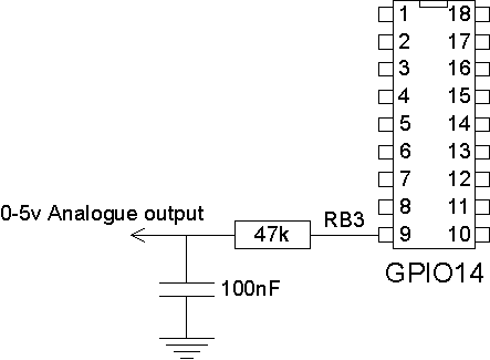
This filter has a worst case output ripple of less than 1 LSB. The output impedance is obviously high at 47k and you may need to buffer this with an op-amp.
Ultrasonic Ranging
Ultrasonic ranging can use either the SRF04 or SRF05 modules. Full timing and
control of up to 2 modules is available.

The diagram above shows the signal connection for connecting two SRF04 ultrasonic rangers to the GPIO14. This also works for the SRF05 if the SRF05s mode pin is unconnected which puts it in SRF04 compatibility mode. The GPIO14 can perform ranging of the SRF04s in uS, Centimeters or Inches. The following commands select the ranging mode:
| Command | Value | Action |
| SET_US | 12 (0x0C) | Set ranging in uS |
| SET_CM | 13 (0x0D) | Set ranging in centimeters |
| SET_IN | 14 (0x0E) | Set ranging in Inches |
To start a ranging, write GET_S4A to the command register for
SRF04(A), or GET_S4B for SRF04(B).
Now you must wait at least 60ms for the ranging to complete. The GPIO14 will not
respond to any further I2C commands whilst it is ranging.
The result of the ranging is placed in the RESULT register and can be read from
there.

The diagram above shows how to connect two SRF05s to the GPIO14.
With the SRF05 mode pin tied to 0v, it operates in a single pin mode where the
trigger and echo pulses both use the same pin.
RB6 and RB7 are unused in the mode and can be used for general purpose I/O.
To start a ranging, write GET_S5A to the command register for SRF05(A), or
GET_S5B for SRF05(B).
Now you must wait at least 60ms for the ranging to complete. The GPIO14 will not
respond to any further I2C commands whilst it is ranging.
The result of the ranging is placed in the RESULT register and can be read from
there.
Changing the I2C Bus Address
This is the LAST thing you should attempt - really! The factory default address
of the GPIO14 chip is 0x40. We strongly recommend you get it working at this address before you try
changing it.
The I2C bus address can be changed to 0x40, 0x42, 0x44, 0x46, 0x48, 0x4A, 0x4C or 0x4E, by writing a specific sequence to register 7, the I2C address change register. The sequence is 0xA0, 0xAA, 0xA5 and then the new address. This sequence must be written to register 7 in four separate I2C bus transactions. You must not read or write to any other registers during this sequence. The new address is stored in EEPROM within the chip and will be active immediately. To prevent confusion, you should then label the chip with its new address.